
Tel:13631651588
E-mail:lijie@szqyxkj.com
Address:Room 309, Building D, Weibaifu Building, Shekou, Nanshan District, Shenzhen
1. Selection principles of triode and MOSFET devices
1. Selection principles of triode and MOSFET devices
1.1 Introduction to triode and MOSFET classification
Type
Type Subdivision
Application Scenario
Triode< br/> RF Signal Transistor
RF Switch and RF Small Signal Amplification
Triode
Ordinary small signal transistor
Small signal loop switch and signal amplifier
Power Loop Switch, Push-Pull Amplification
MOSFET
Small Signal MOSFET
Small Signal Loop Switch< br/> MOSFET
Power MOSFET (<=250v)
AC-DC,DC-DC Power Module
MOSFET
Power MOSFET (600V~650V)
AC-DC Power Module
MOSFET
Power MOSFET (800V~1000V)
AC-DC Power Module, UPS, Inverter
MOSFET
Power MOSFET (1000V~1700V) Air Conditioning Compressor Drive Circuit
MOSFET
Power MOSFET (SIC)>=600V
AC-DC Power Module (High Efficiency)
MOSFET
Power MOSFET (GAN) (100V~600V)
UHF field (above 1Mhz), higher power density application field.
1.1.1 Triode Selection Principle
Efficiency, integration and greening. Emphasis is placed on miniaturization and surface mount.
In recent years, with the development of MOSFETs, in the field of low-power and high-speed switching, MOSFETs are gradually replacing triodes, and mainstream manufacturers in the industry have also reduced their R&D investment in triodes. Investment, the technological development of the device is mainly reflected in the upgrade of the wafer process (6inch wafer to 8inch wafer) and the miniaturization of packaging and surface mount. In addition, compared with ordinary triodes, the main development direction of RF triodes is low-voltage voltage power supply, low noise, high frequency and high efficiency.
The selection principles are as follows:
2) The mainstream miniaturized surface mount devices in the industry are preferred, such as SOT23, STO323, SOT523, etc. For multi-tube applications, dual-tube packages such as SOT363 and SOT563 are preferred.
3) For switch application scenarios, Priority should be given to MOSFET
4) RF transistors are preferably low-voltage power supply, low-noise, high-frequency and high-efficiency devices.
1.1.2 MOSFET selection principle
The general trend of industry technology development is: miniaturization, surface mount, high frequency, High power density, high efficiency, high reliability, integration and greening. Focus on high frequency, high power density, high reliability and integration.
Industry technology development trends are mainly reflected in the evolution and development of MOSFET chip materials, wafer technology, chip technology and packaging technology. The selection principles are as follows:
Plug-in packaged devices at the end of their life cycle (except TO220 and TO247 for energy use) and surface mount devices with SO8 and DPAK packages are prohibited.
For signal MOSFETs, it is recommended to use miniaturized surface mount devices with integrated gate TVS protection.
1) For the power mosfet of Vds<=250v
If the requirements are met, the wing-shaped surface mount package D2PAK with pins can be considered;
Buck upper and lower tube integration solutions are preferred to down tube sourcing down POWERPAK5X6 dual package;
  ; Considering the heat dissipation of the device, the power supply module can choose the mainstream plug-in package TO220
For slow-start and hot-swap applications, please focus on evaluating whether the device works in its safe working area when selecting the device
br/> Switch applications need to start at the same time, hot swap and ORing applications should be selected separately
In the ultra-high frequency field (above 1MHz), GANMOS can be considered instead. This improves efficiency and reduces system area.
2) For high-voltage power MOSFETs with Vds between 600V~650V, it is preferred to use devices with Vds of 650V for AC power modules;
Package According to the heat dissipation and structural design requirements of the power module, it is recommended to select the surface mount device POWERPAK 8X8 and the plug-in TO247. In the future, the surface mount device POWERPAK5X6 can also be considered;
For PFC circuits, MOSFETs with parasitic diodes without fast recovery characteristics (such as INFINEON C3, C6, and P6 series) are preferred. For scenarios with high operating frequencies in the circuit, such as LLC circuits, MOSFETs with parasitic diodes with recovery characteristics (such as INFINEON CFD) are preferred. Series);
For scenarios where power efficiency requirements are not particularly high, some MOSFETs can be replaced with high-speed IGBTs to reduce costs. For high-efficiency modules, SIC MOSFETs can be considered to replace traditional Si MOSFETs to improve power supply efficiency;
For MOSFETs with Vds higher than 800V, if Id is greater than 5A, it is recommended to consider using IGBTs. If the Id is less than 5A, it is recommended to use the industry mainstream package TO247, TO220 or D2PAK;
In principle, depletion JFET is prohibited. choose.
2. Key elements of transistor and MOSFET device selection
2.1. Key elements of transistor selection
There are two functions of amplification and switching. At present, the triode mainly plays the role of switching in our circuit. When choosing a triode, consider the following aspects: parameters, packaging, performance (low drop, low impedance, high magnification, high switching efficiency)
1) Selection of parameters: There are many parameters of the triode. There are no special requirements for the parameters of the triode. The parameters that need to be paid attention to are Vceo, Vcbo, Vebo, Ic(av), Pd, Hef. The more important parameters are Vceo and Ic(av). For the value of Vceo, sometimes the manufacturer will give the value of Vces. The value of Vces cannot be used as Vceo, because Vces=Vcbo>Vceo. If the voltage and current values of the device meet the requirements after derating, Pd can not be considered too much (Pd needs to be considered when the triode is used for amplification, voltage linear conversion and the power of the triode is relatively large).
On the premise of meeting the derating requirements, consider the output current and corresponding dissipated power, breakdown voltage, magnification and other parameters. At the same time, the device with small thermal resistance and high junction temperature should be selected as far as possible.
2) Packaging: The development trend of triode packaging is miniaturization, surface mount, flat feet, and no leads.
The quality of the package is judged by the ratio of the chip area to the package area. The closer the ratio is to 1, the better. The current triode small package is sot883 (DFN1006-3), preferably sot883, sot663, sot23, sot89, sot223, sot666. Since the power requirements of triodes are getting smaller and smaller, small-package triodes are one direction of its introduction. On the premise that the parameters meet the specifications, try to choose small packages.
3) Performance: choose low Vce (sat), low impedance devices. At present, NXP, ON, ZETEX, etc. have launched devices with low saturation voltage drop, which can be given priority when selecting models.
2.2. MOSFET selection key elements
2.2.1 Voltage limit parameters
1) Drain-source breakdown voltage V(BR)DSS: Drain-source breakdown voltage V(BR)DSS is generally the test value at junction temperature Tj=25℃, VGS=0V, ID is hundreds of A, because V(BR) ) DSS and Rds(on) are inversely proportional, so the upper limit of most manufacturers' MOSFETs is 1000V. V(BR)DSS is related to temperature. When Tj increases by 100℃, V(BR)DSS increases linearly by about 10%. Conversely, when Tj decreases, V(BR)DSS decreases in the same proportion. This feature can be regarded as one of the advantages of MOSFET, which ensures that when thousands of cells inside the avalanche breakdown, it is difficult for the avalanche current to be concentrated at a certain point and cause device damage (unlike power transistors).
2) Large rated gate-source voltage VGS
If the voltage is not high, a high electric field will be formed inside, and if the electric field exceeds the bearing capacity of the SiO2 material, breakdown will occur and the device will fail.
The maximum rated gate-source voltage VGS is 20V in most manufacturers' data (generally 10V for low-voltage MOSFETs with low driving voltage). At present, many manufacturers have raised this limit voltage to 30V for high driving voltage MOSFETs. SIC MOSThe FET is mostly between 10V and 25V, and the starting voltage is asymmetric. When selecting, pay attention to the design of the driving part.
2.2.2 Main parameters affecting loss
For MOSFET, when the frequency is less than 100KHz, the proportion of conduction loss is mainly Large. Therefore, the main parameter that affects the loss is the on-state resistance Rds(on). Generally, the Rds(on) value given by the manufacturer is the value under the specified VGS (such as 10V) ID (usually the nominal current value) and Tj (usually 25°C).
For Rds(on), it has the following characteristics: For manufacturers, under the same design and process conditions, if the Rds(on) value of MOSFET is increased, it will lead to Rds(on) rise. The Rds(on) value increases approximately linearly with increasing junction temperature. The result is an increase in loss. For example, the Rds(on) vs. Tj diagram of the IRF640 in the figure below shows that if the junction temperature is 120°C, the Rds(on) value will be 1.8 times that at 25°C. Therefore, the conduction loss I2*Rds(on) will also increase to 1.8 times; compared with Si MOSFET, SiC MOSFET has a wider band gap than Si MOSFET, so its temperature characteristics are significantly better than Si MOSFET. At 150℃, the Rds(on) of SIC MOSFET is only 20% higher than that at 25℃.
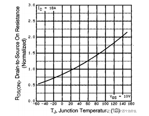
Figure 1 Rds(on) and Tj Relationship Diagram
Relationship with VGS: In order to reduce Rds(on) to   ; Small, at least VGS must be increased to 10V (about 5V for 4V-driven products) before it can be reduced to small. In addition, even if VGS is increased to more than 12V~15V, it will not have much effect on the reduction of Rds(on) (if the use of close to or exceeding the DC rated current in the case of a small duty cycle, it is another matter), Unnecessarily increasing this gate voltage will increase the charging current, increase the drive loss, and easily generate voltage spikes between the gate and the source. Increase the failure probability of gate-source breakdown. Therefore, for general MOSFETs, 12V drive is sufficient.
At the same junction temperature, Rds(on) increases slightly with the increase of ID. This change can be ignored when calculating power consumption. In actual use, if the ID value is increased, the heat generation will increase, it is because the heat dissipation conditions (thermal resistance) remain unchanged, the ID increases, the power consumption P= I2* Rds(on) increases, the junction temperature increases, Rds(on ) increases accordingly, further increasing the power consumption.
In addition, when the frequency exceeds 100KHz, the proportion of switching loss cannot be ignored. At this time, it is necessary to pay attention to the gate charge Qg of the device itself, the output capacitor Coss, and the gate drive resistor pair The effect of switching losses. In particular, the smaller the on-state resistance of the MOSFET, the larger the cell density, the larger the Qg and the Coss, which will increase the switching loss.
Recently, due to the further increase in the application frequency of MOSFETs, in the production of low-voltage and high-current MOSFETs, it is necessary to improve the parasitic Rg inside the MOSFET from the process design to reduce the switching loss of the MOSFET. Increase the applied frequency (or increase the current)
2.2.3 Current Handling Capability Parameters
Limiting Current Handling Capability Final The factor is the maximum allowable junction temperature (usually the manufacturer specifies 150°C). Generally, it is characterized by sustainable DC drain current ID and rated peak current IDM.
1) Sustainable DC drain current ID
Actual allowable Thermal resistance RJC (it depends on the chip packaging material and process level of the device), maximum allowable junction temperature Tj, and mechanical parameters such as case temperature Tc. They satisfy the following formula:
I2* Rds(on)*Rjc=Tjmax-Tc
where Rds(on), Rjc, Tjmax are determined by the device itself The characteristics are determined, and Tc is related to the design, such as heat dissipation conditions, power consumption, etc. (Note: allowable large drain power consumption Pd= I2*Rds(on)=(Tjmax-Tc)/Rjc). The general manufacturer's information gives the ID value at the case temperature, and some manufacturers also give the relationship curve between the large ID and Tc.
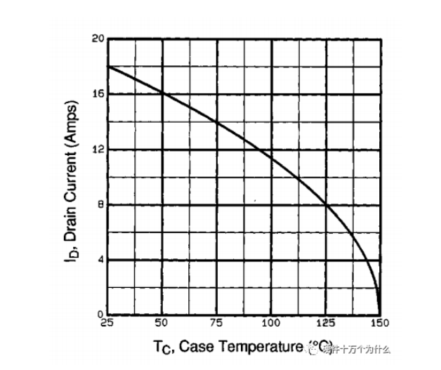
Figure 2 Relationship between ID and Tc
Taking IRF640 as an example, the nominal current is 18A (under Tc=25℃) ), the relationship between its ID and Tc is shown in the figure above. It can be seen from the figure that when the case temperature changes from 25°C to 125°C, the large DC drain current drops from 18A to 8A. It must be noted that the ID at Tc=25°C is only for reference (comparisons between different tubes can be made), because it assumes that the heat dissipation conditions are good enough, and the case temperature is always 25°C (in practical applications, it is not possible at all) ), which is calculated according to the formula I2* Rds(on)*Rjc=Tjmax-Tc. However, in practical applications, due to the limitations of ambient temperature and actual heat dissipation conditions, the case temperature is usually much greater than 25°C, and the high junction temperature is usually maintained at a derating of more than 20°C. Therefore, the allowable DC drain current must be derated with increasing temperature.
2) Rated peak current IDM
If the current pulse or duty cycle is small, it is allowed to exceed the ID value, but its pulse width or duty cycle Subject to maximum allowable junction temperature. The general manufacturer's data stipulates that the rated peak current IDM value at 25°C is four times the ID value, and is obtained at VGS=20V.
2.2.4 Parameters related to gate drive
parasitic capacitance. Therefore, when driving, the capacitor has charging and discharging current and charging and discharging time, which is the root cause of driving loss and switching loss. The switching characteristics of a device are usually measured in Qg.
1) Input capacitor Ciss, reverse transfer capacitor Crss, output capacitor Coss
Parasitic capacitance, therefore, when driving, the capacitor has charging and discharging current and charging and discharging time, which is the root cause of driving loss and switching loss. The switching characteristics of a device are usually measured in Qg.
1) Input capacitor Ciss, reverse transfer capacitor Crss, output capacitor Coss
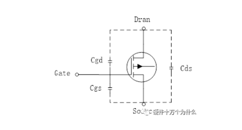
Figure 3 MOSFET parasitic capacitance
As shown above, Ciss=Cgd+Cgs, Crss=Cgd, Coss=Cds+Cgd< br/> 2) The total gate charge Qg
It represents the charging charge required to reach the specified gate voltage during turn-on. It is measured under the specified VDS, ID and VGS (usually 10V) conditions.
Due to the existence of the Maitreya effect, although Cgd is much smaller than Cgs, it plays a larger role in the driving process Therefore, objectively speaking, the Qg of MOSFET is compared to the Ciss Wait to be more accurate.
In addition, there are two parameters of gate charge Qge and gate charge (Mitler charge) Qgd.
The following figure takes IRF640 as an example to illustrate their waveforms.
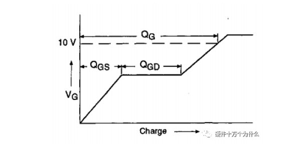
Figure 4 Gate charge and VG
3) Gate resistance Rg, turn-on delay time td(on), rise time tr, The turn-off delay time td(off) and the fall time tf
also describe the switching performance of the device, and are also related to the driving loss of the device. Its specific value is closely related to the test conditions. Be especially careful when comparing different tubes. Otherwise, it is easy to be misled by the manufacturer.
2.2.5 Parameters related to reliability
1) Maximum allowable junction temperature Tjmax
This is reliability It is an important parameter. For MOSFETs, general manufacturers mark it as 150°C, and there are also special semiconductor devices at 125°C and 175°C.
2) Avalanche rating
Due to leakage and distributed inductance and di/dt at turn-off, there may be voltage spikes that force the MOSFET into avalanche In the breakdown region, VDS is clamped at the actual breakdown voltage point, but if the actual entry into the avalanche breakdown region is very short and the energy is very small, the device itself can consume it without damage.
There are three parameters that can characterize this characteristic, that is, the single pulse avalanche energy EAS, the allowable repeated pulse avalanche energy EAS (the pulse width is limited by the large junction temperature), The initial large avalanche current IAR when an avalanche occurs. The avalanche energy rating drops significantly with increasing junction temperature and with increasing inception current when an avalanche occurs.
If there is avalanche when the device is working, please note that in the aging process, since the junction temperature will increase accordingly, the avalanche capability will decrease accordingly. If it drops to a certain extent, the device may be damaged. And this damage usually only presents a certain proportion. (Of course, other reasons may also cause MOSFET damage, such as the magnetic saturation of the transformer under high temperature and high current)
3) Gate leakage current IGSS, drain off-state leakage current IDSS
These two parameters may not be used in specific design, but they limit the quality of the internal process and materials of the device. Although their values may be as small as mA level or uA level, when comparing devices , by testing it as a function of voltage (especially at high temperature)The situation can also be compared to judge the pros and cons of the device.
2.2.6 Parameters related to parasitic source-drain diodes
At this time, it is necessary to examine the parameters of the diode.
1) dv/dt value
When the body parasitic diode is freewheeling, minority holes also participate in conduction, and the concentration is very high, when the diode conducts At the end of the pass cycle, when the external circuit reverses the diode, if the voltage between D and S rises too fast, a part of a large number of minority holes cannot be recombined, causing a current flowing laterally through the body region, which is in the P+ region and the source. The voltage drop formed between the regions N+ may make the parasitic triode turn on, (the drain D is equivalent to the collector of the parasitic NPN triode, P+ is equivalent to the base, the source S is equivalent to the emitter, and the base-emitter has a positive When the voltage drops in the forward direction, due to the large dv/dt, the voltage rises quickly, and there is also a positive voltage between the collector and the emitter, so the parasitic triode is turned on), the current will be concentrated in The device is damaged by thermal breakdown.
2) Other parameters
a. Reverse recovery characteristics, including reverse recovery charge and reverse recovery time. Matching should be considered when freewheeling is used.
b. Current and voltage parameters, there is forward voltage drop VSD, its current parameters IS, ISM are the same as ID, IDM, relative to SI MOSFET, the forward voltage drop of the parasitic diode of SIC MOSFET , this is because the Knee voltage (Knee voltage: point at which diode turn on) of SIC is 3 times that of Si, which is very close to the ratio of their forbidden band widths, so the VSD of SIC MOSFET is about 2.5V, while the Si MOSFET's VSD is about 2.5V. VSD is about 0,8V.
2.2.7 Package
Select a package with the appropriate package style and thermal resistance. Common power MOSFET packages are DPAK, D2PAK, PowerPAK 5X6, PowerPAK 3X3, DirectFET, TO220, TO247, SOT23, SOT323 corresponding to small signal MOSFETs, etc. PowerPAK 8X8, PowerPAK SO8 5X6 Dual, PowerPAK 5X6 dual cool, SO8 Packaged devices are in the exit period in the industry, and are prohibited during selection. DPAK packaged devices are in the saturation period in the industry, and the selection time is limited; plug-in packages are preferred in energy scene applications, such as TO220, TO247.
Phone:13631651588
address:Room 309, Building D, Weibaifu Building, Shekou, Nanshan District, Shenzhen
URL:www.szqyxkj.com
mailbox:lijie@szqyxkj.com

Follow us
2026 Shenzhen Quanyouxing Technology Industry Co., Ltd. Phone:13631651588 ICP:粤ICP备09036100号-2 Technical:华企立方


