
Tel:13631651588
E-mail:lijie@szqyxkj.com
Address:Room 309, Building D, Weibaifu Building, Shekou, Nanshan District, Shenzhen
Preparations for choosing diodes in circuit design
Source: Network Organization Posted in : 2021-11-09 17:11:29
A crystal diode is a P-N junction formed by a P-type semiconductor and an N-type semiconductor. A space charge layer is formed on both sides of the interface, and a self-built electric field is built. When there is no applied voltage, the diffusion current caused by the difference in carrier concentration on both sides of the P-N junction is equal to the drift current caused by the self-built electric field and is in an electrical equilibrium state.
When there is a forward voltage bias outside, the mutual suppression of the external electric field and the self-built electric field makes the current carrying The increase in the diffusion current of the electrons causes a forward current.
When there is a forward voltage bias in the outside world, the mutual suppression of the external electric field and the self-built electric field increases the diffusion current of the carriers and causes the forward current.
When there is a reverse voltage bias outside, the external electric field and the self-built electric field are further strengthened, forming a reverse voltage independent of the reverse bias voltage value within a certain reverse voltage range. towards saturation current.
When the applied reverse voltage is high to a certain level, the electric field strength in the space charge layer of the P-N junction reaches a critical value, resulting in a multiplication process of carriers and a large number of electron holes. Yes, a large reverse breakdown current is produced, which is called the breakdown phenomenon of the diode.
Main parameters of semiconductor diode
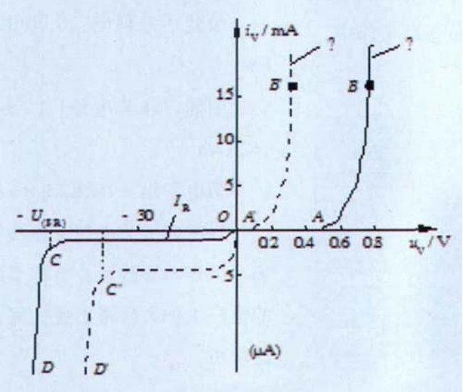
The volt-ampere characteristic curve of the diode is shown in Figure 1.
Figure 1 Diode volt-ampere characteristic curve
1. Reverse saturation leakage current IR
Refers to the current flowing through the diode when a reverse voltage is added across the diode, and the current is related to the semiconductor material and temperature. At room temperature, the IR of silicon tube is nanoamp (10-9A) level, and the IR of germanium tube is microamp (10-6A) level.
2. Rated rectified current IF
refers to the average current value converted from the allowable temperature rise when the diode is running for a long time. At present, the IF value of high-power rectifier diodes can reach 1000A.
3. Large average rectified current IO
In a half-wave rectifier circuit, the large value of the average rectified current flowing through the load resistor. This is a very important value at design time.
4. Large surge current IFSM
Excessive forward current is allowed to flow. It is not a normal current, but an instantaneous current, which is quite large.
5. Large reverse peak voltage VRM
Even if there is no reverse current, as long as the reverse voltage is continuously increased, sooner or later the diode will be damaged. This reverse voltage that can be added is not an instantaneous voltage, but a forward and reverse voltage that is repeatedly added. Since the AC voltage is applied to the rectifier, its maximum value is an important factor specified. The maximum reverse peak voltage VRM refers to the maximum reverse voltage that can be applied to avoid breakdown. Currently high VRM values can reach several thousand volts.
6. Large DC reverse voltage VR
The above-mentioned large reverse peak voltage is the peak voltage that is repeatedly applied, and VR is the value when the DC voltage is continuously applied. For DC circuits, large DC reverse voltages are important to determine allowable and upper limits.
7. High operating frequency fM
Due to the junction capacitance of the PN junction, when the operating frequency exceeds a certain value, its unidirectional conductivity will deteriorate. The fM value of the point-contact diode is higher, above 100MHz; the fM of the rectifier diode is lower, generally not higher than several kilohertz.
8. Reverse recovery time Trr
When the working voltage changes from forward voltage to reverse voltage, the ideal situation of diode operation is that the current can be cut off instantaneously. In practice, there is usually a slight delay. The amount that determines the current cut-off delay is the reverse recovery time. Although it directly affects the switching speed of the diode, it is not necessarily a small value. That is, when the diode is suddenly reversed from conduction, the time required for the reverse current to decay from a large amount to close to IR. This indicator is very important when the high-power switch tube works in the high-frequency switching state.
9. High Power P
A current flows through the diode, which absorbs heat and increases its temperature. High power P is the large value of power. Specifically, the voltage across the diode multiplied by the current flowing through it. This limit parameter is particularly important for Zener diodes and variable resistance diodes.
Semiconductor diode nomenclature
The model number of a semiconductor device consists of five parts, as shown in Figure 2. Such as 2AP9, where "2" means the number of electrodes is 2, "A" means N-type germanium material, "P" means ordinary tube, and "9" means the serial number.
Classification of semiconductor diodes
Semiconductor diodes can be divided into ordinary diodes and special diodes according to their uses. Common diodes include rectifier diodes, detection diodes, Zener diodes, switching diodes, fast diodes, etc.; special diodes include varactor diodes, light-emitting diodes, tunnel diodes, trigger diodes, and laser diodes. The characteristics of several main diodes are as follows:
1. Rectifier diode
The structure of the rectifier diode is mainly a plane contact type, which is characterized by a relatively large allowable current and a relatively high reverse breakdown voltage, but the PN junction capacitance is relatively large. It is generally used in In circuits with low processing frequency. For example, rectifier circuit, clamping circuit, protection circuit, etc. The main factors considered in the use of rectifier diodes are large rectifier current and high reverse working voltage should be greater than the value in actual work.
2. Fast diode
The working principle of fast diodes is the same as that of ordinary diodes, but due to the long reverse recovery time of ordinary diodes in the switching state, about 4 ms to 5 ms, it cannot adapt to high frequency switching circuit requirements. Fast diodes are mainly used in high-frequency rectifier circuits, high-frequency switching power supplies, high-frequency resistance-capacitance absorption circuits, inverter circuits, etc., and their reverse recovery time can reach 10ns. Fast diodes mainly include fast recovery diodes and Schottky diodes.
3. Fast recovery diode (FRD for short): It is a semiconductor diode with good switching characteristics and short reverse recovery time. It is mainly used in switching power supplies, PWM pulse In electronic circuits such as wide modulators and frequency converters, they are often used as high-frequency rectifier diodes, freewheeling diodes or damping diodes. Fast recovery diodes are manufactured by gold-doped, simple diffusion and other processes, which can achieve higher switching speed and higher withstand voltage. The internal structure of the fast recovery diode is different from the ordinary PN junction diode. It belongs to the PIN junction diode, that is, a base region I is added between the P-type silicon material and the N-type silicon material to form a PIN silicon wafer. Because the base region is very thin and the reverse recovery charge is small, the reverse recovery time of the fast recovery diode is short, the forward voltage drop is low, and the reverse breakdown voltage (withstand voltage value) is high. The main application of fast recovery diodesIt is used as a rectifier element in the inverter power supply, amplitude limiting and clamping in high frequency circuits.
4. Schottky diode: also known as Schottky barrier diode (SBD for short), it is based on the barrier layer formed by the contact between metal and semiconductor. The diode is mainly characterized by small forward voltage drop (about 0.45V), short reverse recovery time and small switching loss. It is a low-power, ultra-high-speed semiconductor device used in switching power supplies, inverters, drivers, etc. It can be used as high frequency, low voltage, high current rectifier diode, freewheeling diode, protection diode, or used as rectifier diode and small signal detection diode in microwave communication and other circuits. The Schottky diode is very different from the PN junction diode in structure. Its interior is composed of anode metal (blocking layer made of materials such as molybdenum or aluminum), silicon dioxide (SiO2) electric field elimination material, and N-epitaxial layer. (arsenic material), N-type silicon substrate, N+ cathode layer and cathode metal, etc., a Schottky barrier is formed between the N-type substrate and the anode metal. When a forward bias is applied to both ends of the Schottky barrier (the anode metal is connected to the positive electrode of the power supply, and the N-type substrate is connected to the negative electrode of the power supply), the Schottky barrier layer becomes narrower and its internal resistance becomes smaller. On the contrary, if a reverse bias is applied to both ends of the Schottky barrier, the Schottky barrier layer becomes wider and the internal resistance becomes larger.
Schottky diodes have low withstand voltage and large reverse leakage current. According to this feature, they can be used in high frequency and low voltage circuits. At present, its main application is still in power conversion circuits. The withstand voltage is generally less than 150V, the average current is less than 100A, and the reverse recovery time is between 10 ns and 40 ns.
5. Zener diode: Zener diode, also known as Zener diode or reverse breakdown diode, is the voltage regulator performance shown by the reverse breakdown characteristics of PN junction The fabricated device plays a role in stabilizing the voltage in the circuit. When the diode is reversely broken down, the reverse voltage will not change with the reverse current within a certain reverse current range. Zener diodes are usually made of silicon semiconductor materials by alloying method or diffusion method. It not only has the unidirectional conduction characteristics of ordinary diodes, but also works in reverse breakdown state. When the reverse voltage is low, the Zener diode is turned off; when the reverse voltage reaches a certain value, the reverse current suddenly increases, and the Zener diode enters the breakdown region. At this time, even if the reverse current changes within a large range, The reverse voltage across the Zener diode remains essentially unchanged. When the reverse current increases to a certain value, the Zener diode will be completely broken down and damaged. The characteristic curve of the Zener diode is shown in Figure 3.
Figure 3 Voltage-current characteristic curve of Zener diode
Different Zener diodes can be divided into various types according to package form, current capacity and internal structure. Divided by packaging form, there are three types of Zener diodes in metal casings, glass packaging (referred to as glass packaging) Zener diodes and plastic packaging (referred to as plastic packaging) Zener diodes. There are two types of plastic-encapsulated Zener diodes: lead type and surface mount.
The main parameters of the Zener tube include:
1. The voltage regulator value VZ, the voltage drop across the regulator tube when the current flowing through the regulator tube is a certain value;
2. Voltage temperature coefficient, the temperature coefficient of the voltage regulator value VZ of the Zener tube is a negative temperature coefficient value when VZ is lower than 4V; when the value of VZ is greater than 7V, Its temperature coefficient is positive; when the value of VZ is around 6V, its temperature coefficient is approximately zero. At present, the low temperature coefficient zener tube is made of two zener tubes in reverse series. When the two zener tubes are in the forward and reverse working state, they have different positive and negative temperature coefficients, which can obtain good temperature compensation. .
3. The dynamic resistance rZ indicates the quality of the voltage regulator performance. Generally, the larger the working current, the smaller the rZ; 4. The allowable power consumption PZ is determined by the voltage regulator. The temperature rise allowed by the tube is determined. The PZ value of the low-power voltage regulator tube is 100 mW ~ 1000 mW, and the high-power voltage can reach 50W. 5. Stable current IZ, the current applied when testing the parameters of the Zener tube. When the actual current flowing through the Zener tube is lower than IZ, it can still be regulated, but rZ is larger.
The main purpose of the Zener tube is to stabilize the voltage. When the requirement is not high and the current variation range is not large, the voltage regulator value can be selected and required It is directly connected in parallel with the load for the close zener tube. It is generally used as a reference power supply in a regulated and constant current power supply system, and is also used as a DC level shift in an integrated operational amplifier. Its disadvantages are high noise figure and poor stability.
6. Semiconductor Light Emitting Diodes: Light Emitting Diodes (LEDs) are made of III-IV compounds, such as GaAs (gallium arsenide), GaP (gallium phosphide), GaAsP (phosphorus gallium arsenide) and other semiconductor materials. In addition to the I-N characteristics of the general P-N junction, it also has light-emitting characteristics under certain conditions. Semiconductor light-emitting diodes are electroluminescent devices excited by current, and this phenomenon was discovered in 1923 and did not attract people's attention at that time. With the development of modern technology, new requirements are put forward for light-emitting devices. It is hoped that the light-emitting tube is simple, reliable, long life, low price and miniaturization. Since the 1960s, electroluminescence research has been very active.
LED structures vary by application and material doping. LEDs used for visible light indication and display require structure optimization to achieve high efficiency; LEDs used for optical communication, the emission wavelength must be in the window area where the fiber exhibits low loss, and high radiation high power Coupled into the fiber, in addition to need to have a larger modulation capacity.
The main features of LED are that it works under low voltage (below 2 volts) and low current (tens of mA to 200 mA), with low power consumption, small size, It can be directly connected with solid circuit, and is stable, reliable, long life (105-106 hours), and cheap. In addition, LED modulation is convenient, and the light output can be modulated by modulating the driving current.
LED can be used as indicator light, alphanumeric display, optocoupler device, light source of optical communication system, etc. There are two types of LEDs used as indicator lights: radial lead structure and axial lead structure. The former is small in size and low in price, and is suitable for installation on a printed circuit board (PCB); the latter can be installed on the instrument panel or directly on the PCB. Designed for PCB small LED indicators, compatible with transistors and integrated circuits, used to indicate circuit status and faults; alpha-numeric display LEDs are used in digital displays of pocket calculators, digital watches and electronic meters, and more Displayed for seven segments. For desktop calculators, the display is often a full alpha-numeric 35-dot matrix with LEDs arranged in a 7x5 array. The 35-dot matrix is expensive and the driving circuit is complex; LEDs used in optical communication systems require good directivity. The two main light sources suitable for optical communication applications are high-radiance LEDs and semiconductor injection lasers, which are widely used in medium and Light source for short-range optical communication systems. In addition, LEDs are also used in the fields of information processing, image transmission, ranging and sensing; LEDs used as optical coupling devices GaAs (or GaAsP) are combined with Si-PN junction detectors to make many new devices for Optical-to-electrical and electrical-to-optical conversion, commonly referred to as optocoupler devices. Well known are optocoupler isolators, which are high speed, reliable and provide electrical isolation up to 2.5 kV. The automobile ignition device adopts the optical coupling device, which is fuel-efficient, easy to start, and works smoothly.
Driven by the emerging application market, the application field of LED has developed from simple electrical indicator lights and LED displays to LCD backlights, landscape lighting, interior decoration lights and other fields. Due to the characteristics of long life, no pollution and low power consumption of LEDs, LEDs will gradually replace fluorescent lamps and incandescent lamps as the next generation of green lighting sources in the future. Indoor lighting will be LED applications with market scale and development potential. The LED display screen can be divided into single-color, double-color and full-color display according to the color. The LED full-color display is composed of RGB three primary color LEDs.
7. Laser diode: The laser diode is essentially a semiconductor diode. According to the PN junction material, the laser diode can be divided into homojunction and single heterojunction (SH). , double heterojunction (DH) and quantum well (QW) laser diodes. There are two commonly used laser diodes: PIN photodiodes. When it receives optical power to generate photocurrent, it will bring quantum noise; avalanche photodiode. It is able to provide internal amplification and transmit longer distances than PIN photodiodes, but with greater quantum noise. In order to obtain a good signal-to-noise ratio, a low-noise pre-amplifier and a main amplifier must be connected behind the photodetection device. Compared with lasers, laser diodes have the advantages of high efficiency, small size, and long life. The disadvantages are low output power (generally less than 2mW), poor linearity, and poor monochromaticity, so there are many applications in cable TV systems. Restricted, unable to transmit multi-channel and high-performance analog signals. Now, laser diodes have been widely used in low-power optoelectronic devices such as optical disc drives of computers and print heads of laser printers.
The common parameters of semiconductor laser diodes are: wavelength, threshold current Ith, operating current Iop, vertical divergence angle, horizontal divergence angle and monitoring current Im, etc.
Detection method of diode
1. Detection of ordinary diodes
The polarity of the diode is usually marked on the case, and the polarity can also be judged by measuring its forward and reverse resistance with a multimeter resistance gear. Put the multimeter in the R×100 or R×1k(Ω) block (the current in the R×1 block is too large, and the voltage in the R×10k(Ω) block is too high, which will easily damage the tube), the test diagram is shown in Figure 4
Figure 4 Schematic diagram of a simple test diode with a multimeter, in which (a) small resistance; (b) large resistance
2. Detection of ordinary light-emitting diodes
(1) Multimeter detection method. Using a pointer-type multimeter with a ×10kΩ block can roughly judge the quality of the light-emitting diode. In normal conditions, the forward resistance of the diode is tens to 200kΩ, and the reverse resistance is ∝. If the forward resistance value is 0 or ∞, and the reverse resistance value is small or 0, it is easy to damage. With this detection method, the luminescence cannot be seen.
(2) External power measurement. The optical and electrical characteristics of light-emitting diodes can be measured more accurately with a 3V stabilized voltage source or a dry battery and a multimeter. To this end, the circuit can be connected as shown in Figure 5. If the measured VF is between 1.4V and 3V, and the light-emitting brightness is normal, it can be shown that the light-emitting is normal. If VF=0 or VF≈3V is measured, and no light is emitted, it means that the LED is broken.
Figure 5 External power supply to measure LED characteristics
3. Detection of infrared LEDs
Because the infrared light emitted by the infrared light-emitting diode is 1μm~3μm infrared light, the human eye cannot see it. Usually, the emission power of infrared light-emitting diodes is only a few mW, and the angular distribution of the luminous intensity of different types of infrared LEDs is also different. The forward voltage drop of infrared LED is generally 1.3μV ~ 2.5V. Since the infrared light-emitting diode emits invisible light, the above method can only determine whether the forward and reverse electrical characteristics of the PN junction are normal, but cannot determine the light-emitting condition. For this, prepare a photosensitive device as a receiver.
Diode selection
The following main parameters should be considered when selecting diodes in circuit design:
1. Positive features
When the forward voltage at both ends is very small, the diode does not conduct in a "dead zone" state; when the forward voltage exceeds a certain value, the diode begins to conduct, and the current increases with The voltage increases continuously. Diodes of different materials have different starting voltages. The silicon tube is about 0.5V to 0.7V, and the germanium tube is 0.1V to 0.3V.
2. Reverse feature
When the reverse voltage is applied across the diode, the reverse current is very small. When the reverse voltage gradually increases, the reverse current basically remains unchanged. Diodes of different materials have different reverse currents, silicon tubes are about 1 microamp to tens of microamps, and germanium tubes can be as high as hundreds of microamps. The reverse current is greatly affected by temperature changes, and the stability of germanium tubes is slightly worse than that of silicon tubes.
3. Breakdown characteristics
When the reverse voltage increases to a certain value, the reverse current increases sharply, which is called reverse breakdown. The reverse breakdown voltage value varies greatly depending on the device structure, process and material, from 1 volt to several hundred volts, and even as high as thousands of volts.
4. Frequency characteristics
Due to the existence of junction capacitance, when the frequency is high to a certain extent, the capacitance is so small that the PN junction is short-circuited, causing the diode to lose unidirectional conductivity and cannot work. The larger the PN junction area, the larger the junction capacitance, and the less the diode can work at high frequencies.
Ordinary diodes are mainly used for rectification, detection, frequency mixing, switching, voltage regulation, etc., and play an important role in many circuits. Special diodes such as light-emitting diodes have greatly expanded their application fields due to technological progress. In terms of quantity, with the strong domestic manufacturing capacity, indicator lights are still the major application of LED, and the consumption accounts for half of the LED market consumption. However, because the indicator lights are mostly ordinary brightness LEDs, after years of development, the output is very large and a buyer's market has long been formed. The LED market in the indicator light field has grown slowly. Under the environment of energy saving and emission reduction, governments of various countries have issued policies to promote the entry of LED lamps into the general lighting market, and indoor lighting will become an application of LED with potential for development. In addition, the display screen market, the backlight market of digital equipment and the automotive lamp market will become the main application markets for LEDs in the foreseeable future.
Phone:13631651588
address:Room 309, Building D, Weibaifu Building, Shekou, Nanshan District, Shenzhen
URL:www.szqyxkj.com
mailbox:lijie@szqyxkj.com

Follow us
2026 Shenzhen Quanyouxing Technology Industry Co., Ltd. Phone:13631651588 ICP:粤ICP备09036100号-2 Technical:华企立方


