
Tel:13631651588
E-mail:lijie@szqyxkj.com
Address:Room 309, Building D, Weibaifu Building, Shekou, Nanshan District, Shenzhen
MOS tube drive circuit design, how to make MOS tube turn on and off quickly?
Source: Network Organization Posted in : 2021-11-08 16:10:23
About the design of the MOS tube drive circuit, this article talks about how to make the MOS tube turn on and off quickly.
It is generally believed that MOSFETs (MOS tubes) are voltage-driven and do not require driving current. However, there is a junction capacitance between the G pole and the S pole of the MOS tube, which makes driving the MOS less simple.
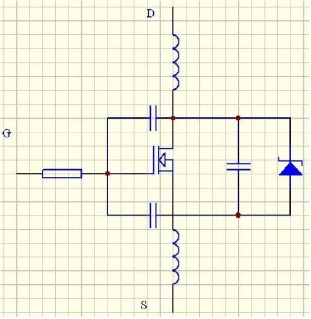
The three capacitors in the figure below are the junction capacitance of the MOS transistor, and the inductance is the parasitic inductance of the circuit trace:
If the requirements such as ripple, EMI and inrush current are not considered, the faster the switching speed of the MOS tube, the better. Because the shorter the switching time, the smaller the switching loss, and in the switching power supply, the switching loss accounts for a large part of the total loss, so the quality of the MOS tube drive circuit directly determines the efficiency of the power supply.
How to turn on and off the MOS tube quickly?
For a MOS tube, if the time it takes to pull the voltage between GS from 0 to the turn-on voltage of the tube is shorter, the faster the MOS tube will turn on. Similarly, if the time for reducing the GS voltage of the MOS tube from the turn-on voltage to 0V is shorter, the faster the MOS tube is turned off.
From this, we can know that if we want to pull the GS voltage up or down in a shorter time, we need to give the gate of the MOS transistor a larger instantaneous drive current.
The commonly used PWM chip output directly drives the MOS or uses a triode to amplify and then drives the MOS. In fact, there is a big defect in the instantaneous drive current.
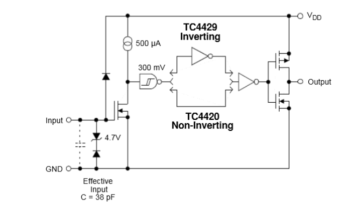
A better way is to use a dedicated MOSFET driver chip such as TC4420 to drive the MOS tube. This type of chip generally has a large instantaneous output current and is also compatible with TTL level. Input, the internal structure of the MOSFET driver chip is as follows:
MOS driver circuit design needs attention:
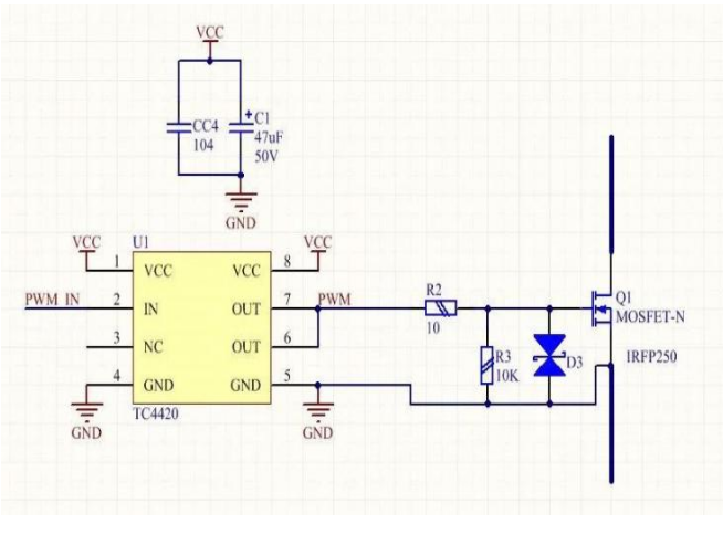
Because the drive line traces will have parasitic inductance, and the parasitic inductance and the junction capacitance of the MOS tube will form an LC oscillator circuit, if the output of the driver chip is directly connected to the MOS If the gate is connected to the gate, there will be a great shock on the rising and falling edges of the PWM wave, which will cause the MOS tube to heat up rapidly or even explode. The general solution is to connect a resistor of about 10 ohms in series with the gate to reduce the Q value of the LC oscillator circuit. Make the shock decay quickly.
Because of the high input impedance of the gate of the MOS tube, a little static electricity or interference may cause the MOS tube to be misconnected, so it is recommended to connect the G pole and the S pole of the MOS tube in parallel. A 10K resistor to reduce input impedance.
If you are worried about the interference coupling on the nearby power line, which will cause instantaneous high-voltage breakdown of the MOS tube, you can connect a TVS transient suppression diode of about 18V in parallel between GS.
TVS can be considered as a fast-response Zener tube, its instantaneous power can be as high as several hundred to kilowatts, and it can be used to absorb instantaneous interference pulses.
In summary, MOS tube driver circuit reference:
Wiring design of MOS transistor driver circuit:
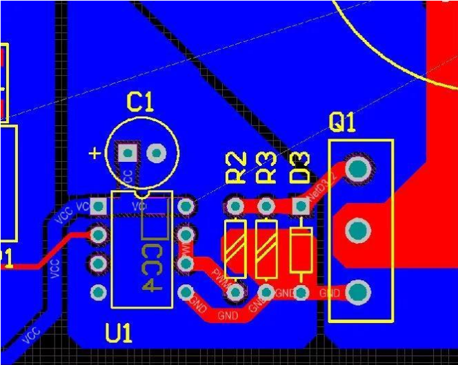
The loop area of the MOS transistor drive circuit should be as small as possible, otherwise it may introduce external electromagnetic interference.
The bypass capacitor of the driver chip should be as close as possible to the VCC and GND pins of the driver chip, otherwise the inductance of the trace will greatly affect the instantaneous output current of the chip.
Common MOS transistor drive waveform:
If there is such a round waveform, just wait for the nuclear explosion. For a large part of the time, the tube works in the linear region, and the loss is extremely large.
Generally, in this case, the wiring is too long, the inductance is too large, and the gate resistance can't save you. You can only redraw the board.
Severely disfigured square wave with high frequency ringing:
The vibration is severe on the rising and falling edges. In this case, the tube generally dies instantly, which is similar to the previous one and enters the linear region.
The reason is similar, mainly the wiring problem. Fat and round fat pig waves.
The rising and falling edges are extremely slow due to impedance mismatch.
The chip drive capability is too poor or the gate resistance is too large.
Resolutely change the driver chip with high current, and adjust the gate resistance to a small one.
The swollen face is filled with sine-shaped triangle waves born from square waves:
The impedance of the drive circuit is too large. This is the sure-kill wave of the tube. The solution is the same as above.
Popular faces, cute square waves:
The high and low levels are distinct, and the level can be called level at this time, because it is flat. The edge is steep, the switching speed is fast, the loss is very small, and the vibration is slightly acceptable.
Square and handsome wave, no ringing, no spikes and no wireless loss, this is the most perfect waveform.
Phone:13631651588
address:Room 309, Building D, Weibaifu Building, Shekou, Nanshan District, Shenzhen
URL:www.szqyxkj.com
mailbox:lijie@szqyxkj.com

Follow us
2025 Shenzhen Quanyouxing Technology Industry Co., Ltd. Phone:13631651588 ICP:粤ICP备09036100号-2 Technical:华企立方


