
Tel:13631651588
E-mail:lijie@szqyxkj.com
Address:Room 309, Building D, Weibaifu Building, Shekou, Nanshan District, Shenzhen
Schottky diode internal structure
Source: Network Organization Posted in : 2021-10-27 17:18:08
Schottky diode internal structure
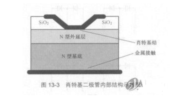
Schottky diodes, also known as Schottky barrier diodes (SBD for short), are made of metal and The diode based on the barrier layer formed by the semiconductor contact is shown in Figure 1. Its main characteristics are that the forward voltage drop is small (about 0.45V), the reverse recovery time is short and the switching loss is small. It is a low power consumption , Ultra-high-speed semiconductor devices. The Schottky diode is very different from the PN junction diode in terms of structure. Its interior is composed of anode metal (blocking layer made of molybdenum or aluminum and other materials), silicon dioxide (SiO2) electric field elimination material, N- It consists of epitaxial layer (arsenic material), N-type silicon substrate, N cathode layer and cathode metal, as shown in Figure 1. A Schottky barrier is formed between the N-type substrate and the anode metal. When a forward bias is applied to both ends of the Schottky barrier (the anode metal is connected to the positive electrode of the power supply, and the N-type substrate is connected to the negative electrode of the power supply), the Schottky barrier layer becomes narrower and its internal resistance becomes smaller; otherwise, if When a reverse bias is applied to both ends of the Schottky barrier, the Schottky barrier layer becomes wider and its internal resistance becomes larger.
Schottky diode structure and internal circuit
The problem with Schottky diodes is that the withstand voltage is relatively low and the reverse leakage current is relatively large. The general level of Schottky diodes currently used in power conversion circuits is that the withstand voltage is below 150V, the average current is below 100A, and the reverse recovery time is 10-40ns. Schottky diodes are ideal for applications in high frequency and low voltage circuits.
Schottky diode structure and internal circuit
1. Schottky diode structure
Figure 13-3 is a schematic diagram of the internal structure of a Schottky diode. Schottky diodes have lower series resistance and stronger nonlinearity, making them suitable for use in RF circuits.
Schottky diode structure and internal circuit
After some metals come into contact with the N-type semiconductor material, electrons will diffuse from the N-type semiconductor material into the metal to form a depletion layer in the semiconductor material, which has the same characteristics as conventional PN The junction is similar, and the structure in which the metal and semiconductor materials contact to form a PN junction-like barrier is called a Schottky junction.
When a forward bias is applied to both ends of the Schottky barrier (the anode metal is connected to the positive pole of the power supply, and the N-type substrate is connected to the negative pole of the power supply), the Schottky barrier The layer becomes narrower and its internal resistance becomes smaller. If a reverse bias is applied to both ends of the Schottky barrier, the Schottky barrier layer will become wider and its internal resistance will increase, as shown in Figure 13-4.
Schottky diode structure and internal circuit
2. The internal circuit of the Schottky diode?
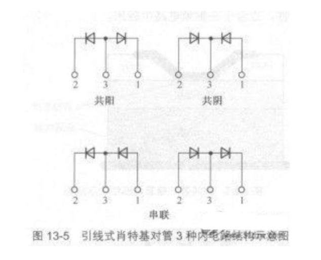
The lead-type Schottky pair tube has a common anode (the positive poles of the two tubes are connected), a common cathode (the negative poles of the two tubes are connected) and a series connection (the positive pole of a diode is connected to each other) The negative pole of the other diode) 3 ways to lead out the pins. JRC2352 Figure 13-5 is a schematic diagram of the circuit structure in the lead-type Schottky pair tube.
Schottky diode structure and internal circuit
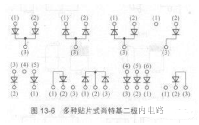
SMD Schottky diodes are available in single, double and triple packages, and there are more than 10 specific forms of internal circuits. Figure 13-6 shows the internal circuits of various SMD Schottky diodes.
Schottky diode structure and internal circuit
Phone:13631651588
address:Room 309, Building D, Weibaifu Building, Shekou, Nanshan District, Shenzhen
URL:www.szqyxkj.com
mailbox:lijie@szqyxkj.com

Follow us
2025 Shenzhen Quanyouxing Technology Industry Co., Ltd. Phone:13631651588 ICP:粤ICP备09036100号-2 Technical:华企立方


